|
Switching DC power supply
Switching DC power supply
D.E.V.I.C.E. is a comprehensive engineering encyclopedia, that includes:
- industry terms used by manufacturers of electronic, test and measurement equipment;
- standards, interfaces and units of quantities;
- multifunctional engineering calculations for circuits, electronic components, connectors, optoengineering, unit converters and more;
- measurement software;
- personality section, about outstanding scientists and inventors;
- historical events from the world of measurements, electronics, physics, chemistry, etc.;
- measurement fun facts.
T&M Atlantic created and maintains this service to better explain the functionality of the instruments it offers and provide general concepts about physical quantities and technological processes. We use tools like video and animation to bring words and images to life and explain boring terms in a way that's easy to understand. Our numerous calculators really help engineers and students in their work and studies.
D.E.V.I.C.E. on Request
If you are searching for a particular term or definition, please contact us and our engineers will be glad to explain it to you.
A switching DC power supply, also known as a Switched-Mode Power Supply (SMPS), is an electronic device that converts electrical power by rapidly turning an input voltage on and off using high-frequency switching technology.
Switching DC Power Supplies Key Advantages
- High efficiency: They typically operate at 80% to 95% efficiency because the switching transistors spend very little time in the "active" state where heat is generated.
- Wide input range: Switching DC power supplies can handle a wide range of input voltages (e.g., 90V – 264V AC), making them suitable for international use without manual switches.
- Compact and lightweight: Because they operate at high frequencies, they use much smaller and lighter transformers and capacitors than linear power supplies.
Typical Switching DC Power Supply with Two Output Voltages
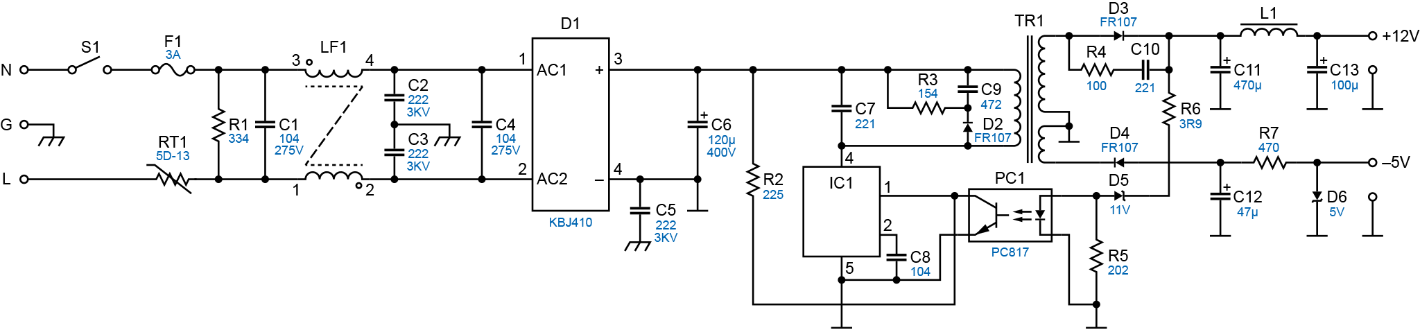
The presented circuit is a typical flyback DC power supply with two output voltages: +12V and -5V. The circuit consists of the following functional blocks:
- Input filter and protection:
- S1 (Switch) and F1 (3A Fuse): Provide on/off control and overcurrent protection.
- RT1 (Negative Temperature Coefficient Thermistor, NTC): Limits the inrush current at turn-on, protecting the rectifier and capacitors. When the power supply is turned on, it presents high resistance, which limits the current surge. As it heats up, its resistance drops, allowing for normal operation.
- LF1 (Line Filter, EMI/RFI): Together with capacitors C1, C2, C3, C4, C5, it suppresses electromagnetic interference (both common mode and differential mode).
- R1 (334 Ω Resistor): Leakage resistor for C1.
- Rectifier and smoothing capacitor (DC Bus Section):
- D1 (AC1, AC2 — Diode bridge KBJ410): Converts alternating mains voltage into pulsating direct voltage.
- C6 (Electrolytic capacitor 120µF, 400V): Smoothes out the ripple of the rectified voltage, forming a high DC bus.
- Key cascade and control:
- IC1 (PWM Controller IC): The main control element. Generates pulse-width modulation (PWM) to control the switching transistor (often built-in or external, shown here as part of IC1).
- TR1 (Pulse Transformer): Provides galvanic isolation between the primary (mains) and secondary (low voltage) parts and converts energy.
- R2, C7: Elements related to IC1 power supply and start-up.
- R3, C9, D2 (RCD Snubber Circuit): Protects the switching transistor from voltage spikes when it is turned off by dissipating excess energy stored in the leakage inductance of transformer TR1.
- Feedback and stabilization:
- PC1 (Optocoupler PC817): Transfers output voltage information from the secondary side to controller IC1 on the primary side, providing galvanically isolated feedback to stabilize the output voltage.
- D5, R5, R7 and D6 (on the -5V side): Part of the feedback circuit (on the secondary side).
- Output cascades (Secondary Side):
- Diodes D3 and D4 (FR107 - fast/ultrafast diodes): Rectify the pulse voltage received from the secondary windings of TR1.
- D3 for the +12V circuit.
- D4 for the -5V circuit. Obviously, D4 is connected to the winding that generates a negative voltage relative to the ground wire.
- Capacitors C10, C11, C12, C13 and Inductor L1: Form LC filters to smooth out high frequency ripple after rectifiers D3/D4, providing clean DC voltage at the output.
- R4, R6 - smoothing filter elements.
Flyback Converter Operating Principle
The flyback converter is one of the most common and simple switched-mode power supply (SMPS) topologies, particularly suitable for low to medium power applications, as well as for providing galvanic isolation and multiple output voltages (as in our diagram: +12V and -5V). The operating principle is based on two main phases (modes): energy accumulation and energy transfer.
Accumulation Phase (IC1 ON)
When IC1 turns on the internal switching transistor (or external MOSFET):
- Storage: Energy from the high voltage DC bus (C6) enters the primary winding of transformer TR1.
- Transformer as inductor: In this phase, transformer TR1 acts as an inductor. It stores energy in its magnetic field.
- Secondary Side blocking: The winding directions of TR1 are chosen such that when voltage is applied to the primary winding, a reverse-polarity voltage is induced on the secondary windings. This voltage blocks the output diodes (D3 and D4), preventing them from conducting current.
- Output power: The load at the output is now fed by the energy stored in the output capacitors (C11, C13, C12) during the previous cycle.
Transmission Phase (IC1 OFF)
When IC1 turns off the key transistor:
- Field collapse: The magnetic field stored in the TR1 core begins to collapse.
- Voltage inversion: Due to the collapse of the field, the polarity of the voltage on all windings (including the primary and secondary) instantly changes to the opposite.
- Rectification: The voltage on the secondary windings becomes of such polarity that it opens the output diodes (D3 and D4).
- Energy transfer: The energy stored in the core is transferred to the secondary side, charging the output capacitors (C11, C13, C12) and powering the load.
- Multiple outputs: Since each secondary winding transfers power independently through its own diode (D3 for +12V, D4 for -5V), the converter easily generates multiple isolated voltages, including negative ones (as shown in our schematic).
Control (Stabilizing)
Controller IC1 uses Pulse Width Modulation (PWM) to stabilize the output voltage:
- The output voltage is measured and this information is passed back to IC1 via optocoupler PC1, providing galvanic isolation.
- If the output voltage drops, IC1 increases the duty cycle of the PWM signal (i.e., increases the time the transistor is on). This allows more energy to accumulate in TR1, resulting in an increase in the output voltage.
- If the output voltage is too high, IC1 reduces the PWM duty cycle, reducing the stored and transferred energy.
PC1 (the PC817 optocoupler) provides galvanically isolated feedback. It transfers output voltage level information from the secondary (low-voltage) side to the IC1 controller on the primary (mains) side, allowing IC1 to accurately maintain output stability without compromising isolation.
Flyback Converter Key Advantages
- Simplicity: One of the simplest topologies, requiring a minimum number of components (especially on the primary side).
- Galvanic isolation: Provided by transformer TR1, which is critical for safety.
- Multiple outputs: Easily generates multiple voltages (both positive and negative) using additional secondary windings.
Possible PWM Controller ICs for IC1
To implement controller IC1 in a flyback converter, specialized PWM controller ICs are used. These are divided into two main types:
- External switch controllers: Require an external power MOSFET.
- Integrated switch (FET) controllers: Include a power transistor directly into the IC package.
Here are some common examples that could be used for IC1 in our schematic.
Integrated MOSFETs (Flyback Switchers / VIPer)
These chips simplify the design by integrating the control and power switches. They are ideal for low- and medium-power circuits (up to ~100W) and match the compact size of our design.
- TNY series (TinySwitch from Power Integrations):
- Description: The TinySwitch family (e.g., TNY26x or TNY27x) uses a simple architecture. They often have only 4–8 pins, as in our schematic, where IC1 has 5 pins.
- Applicability to the schematic: Pin 1 can be the FEEDBACK input (feedback from PC1), pin 5 can be the SOURCE (ground), and the other pins can be the DRAIN (high-voltage drain connected to TR1). The lack of an external MOSFET makes this series a very likely candidate.
- VIPer series (for example, VIPer12A, VIPer22A from ST):
- Description: Similar to TinySwitch, these chips combine a controller and a high-voltage MOSFET. They are popular due to their built-in protection mechanisms.
- Applicability to the schematic: Their topology and pinout often match the requirements of a flyback converter, making them also suitable for implementing IC1.
Switching (SMPS) Power Supplies Application Examples
- Personal computers (PC) / servers: ATX and similar power supplies that require multiple different voltages (+12V, +5V, +3.3V, -12V, etc.) to power the motherboard, processor, hard drives, and peripherals.
- Telecommunications equipment: Power supplies for routers, modems, network switches and VoIP devices where high efficiency, compactness and galvanic isolation are important.
- Industrial automation: Powers PLC controllers, sensors, actuators, and operator panels that often require stable +24V or other voltages, while this dual-polarity supply can power operational amplifiers or specialized interfaces.
Switching vs. Linear Power Supplies
|
Feature
|
Switching (SMPS) Power Supplies
|
Linear Power Supplies
|
|
Efficiency
|
High (≥80%)
|
Low (30 – 60%)
|
|
Noise
|
Higher electrical noise (EMI)
|
Low
|
|
Heat
|
Low
|
High
|
|
Size & weight
|
Small and lightweight
|
Large and heavy
|
Back to the list
4 Search by section
D.E.V.I.C.E. services
|
|