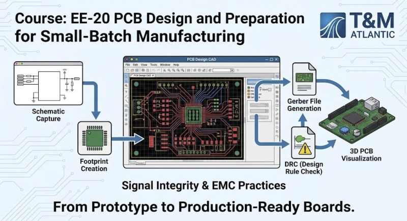
Moving from a functional breadboard circuit to a custom-designed printed circuit board is a vital milestone for any electronics developer. This course provides comprehensive training in modern CAD layout tools, routing standards, signal integrity, and manufacturing file generation.
Objective and Audience
This course guides participants through professional printed circuit board (PCB) design, schematic capture, component footprint creation, multi-layer routing rules, and preparation of manufacturing data (Gerber/ODB++) for modern PCB fabrication houses.
The course is intended for hardware designers, makers, and students looking to turn breadboard prototypes (such as those from EE-31) into reliable, production-ready circuit boards. Completion of EE-3 Basics of Electronics and EE-4 Basics of manual soldering provides useful preparation.
Proposed Format
Ten 90-minute lessons, totaling 15 instructional hours. Interactive sessions combining CAD software walkthroughs (e.g., KiCad / Altium Designer) with design rule checks (DRC) and layout optimization.
Learning Outcomes
By the end of the course, participants will be able to:
- Draw clear, hierarchical electrical schematics and assign correct standard component footprints.
- Design single, double, and multi-layer PCBs following proper trace width, clearance, and copper pour guidelines.
- Implement basic Electromagnetic Compatibility (EMC) and signal integrity practices (ground planes, decoupling capacitors).
- Generate production-ready Gerber files, drill files (excellon), and Bill of Materials (BOM) for fabrication factories.
Lesson Plan
- Introduction to PCB Design Flow:
Overview of CAD tools, schematic capture standards, and project structure.
- Schematic Design Best Practices:
Symbol creation, pin naming, net labels, hierarchical blocks, and ERC checks.
- Footprints and Component Libraries:
Managing pad stacks, 3D models, courtyard definitions, and custom footprint design.
- Board Setup and Constraints:
Defining board outlines, layer stacks (2-layer, 4-layer), track widths, and clearance rules (DRC).
- Placement Strategy & Routing Basics:
Component grouping, thermal management, critical signal routing, and power distribution.
- Ground Planes and Signal Integrity:
Solid ground planes, split planes, return paths, and mitigating noise coupling.
- Decoupling and Power Filtering:
Placing bypass capacitors, managing high di/dt loops, and power rail integrity.
- Design Rule Check (DRC) & Verification:
Running automated checks, clearance verification, and 3D collision inspection.
- Manufacturing Outputs:
Generating Gerber files, Pick-and-Place coordinates, drill files, and BOM generation.
- Final Project Review:
Designing a complete multi-sensor microcontroller board from schematic to manufacturing package export.
Back to the section
|